- 您现在的位置:买卖IC网 > Sheet目录314 > AT93C86AY6-10YH-1.8 (Atmel)IC EEPROM 16KBIT 2MHZ 8MAP
�� �
�
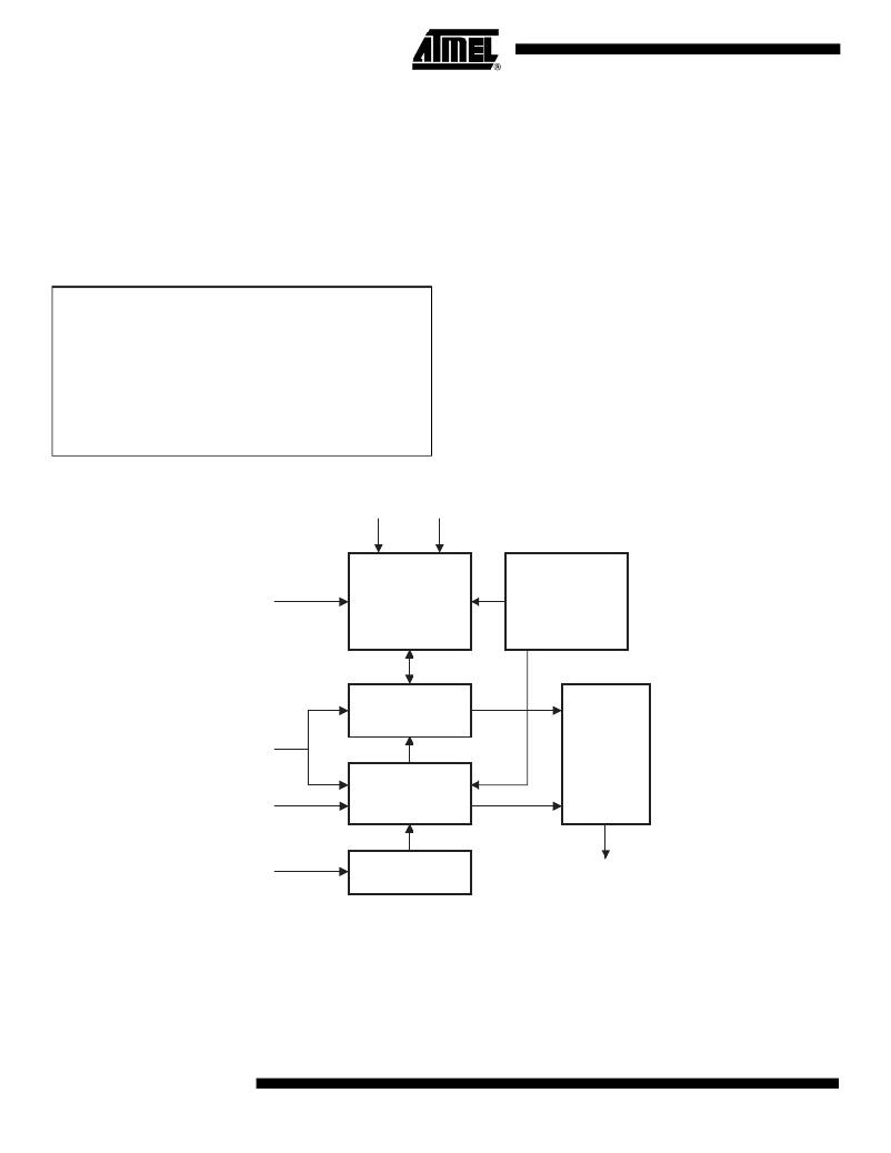
�The� AT93C86A� is� enabled� through� the� Chip� Select� pin� (CS),� and� accessed� via� a� three-�
�wire� serial� interface� consisting� of� Data� Input� (DI),� Data� Output� (DO),� and� Shift� Clock�
�(SK).� Upon� receiving� a� Read� instruction� at� DI,� the� address� is� decoded� and� the� data� is�
�clocked� out� serially� on� the� data� output� pin� DO.� The� Write� cycle� is� completely� self-timed�
�and� no� separate� Erase� cycle� is� required� before� Write.� The� Write� cycle� is� only� enabled�
�when� the� part� is� in� the� Erase/Write� Enable� state.� When� CS� is� brought� “high”� following�
�the� initiation� of� a� Write� cycle,� the� DO� pin� outputs� the� Ready/Busy� status� of� the� part.� The�
�AT93C86A� is� available� in� a� 2.7V� to� 5.5V� version.�
�Absolute� Maximum� Ratings*�
�Operating� Temperature� ......................................?� 55� °� C� to� +125� °� C�
�Storage� Temperature� .........................................?� 65� °� C� to� +150� °� C�
�Voltage� on� any� Pin�
�with� Respect� to� Ground� ........................................� ?� 1.0V� to� +7.0V�
�Maximum� Operating� Voltage� ..........................................� 6.25V�
�DC� Output� Current........................................................� 5.0� mA�
�Figure� 1.� Block� Diagram�
�Vcc�
�GND�
�*NOTICE:�
�Stresses� beyond� those� listed� under� “Absolute�
�Maximum� Ratings”� may� cause� permanent� dam-�
�age� to� the� device.� This� is� a� stress� rating� only� and�
�functional� operation� of� the� device� at� these� or� any�
�other� conditions� beyond� those� indicated� in� the�
�operational� sections� of� this� specification� is� not�
�implied.� Exposure� to� absolute� maximum� rating�
�conditions� for� extended� periods� may� affect�
�device� reliability�
�MEMORY� ARRAY�
�ORG�
�DI�
�2048� x� 8�
�OR�
�1024� x� 16�
�DATA�
�REGISTER�
�ADDRESS�
�DECODER�
�OUTPUT�
�BUFFER�
�MODE�
�DECODE�
�CS�
�LOGIC�
�SK�
�CLOCK�
�GENERATOR�
�DO�
�Note:�
�2�
�When� the� ORG� pin� is� connected� to� Vcc,� the� x� 16� organization� is� selected.� When� it� is� connected� to� ground,� the� x� 8� organization�
�is� selected.� If� the� ORG� pin� is� left� unconnected� and� the� application� does� not� load� the� input� beyond� the� capability� of� the� internal� 1�
�Meg� ohm� pullup,� then� the� x� 16� organization� is� selected.�
�AT93C86A�
�3408H–SEEPR–1/07�
�发布紧急采购,3分钟左右您将得到回复。
相关PDF资料
ATAVRBFLY
KIT EVALUATION AVR BUTTERFLY
ATAVRXBNDL
XMEGA XPLAIN AND DISPLAY MODULE
ATDH2222
ADAPTER FOR ATDH2200 20PLCC
ATDH2225
CABLE ISP FOR AT17
ATDH2227
ADAPTER FOR ATDH2200 44PLCC
ATEVK1101
KIT DEV/EVAL FOR AVR32 AT32UC3B
ATF15XXDK3-SAX20
KIT DEV 20TSSOP ADAPTER ATF15XX
ATJTAGICE2
AVR ON-CHIP D-BUG SYSTEM
相关代理商/技术参数
AT93C86AY6-10YH-1.8 SL383
制造商:Atmel Corporation 功能描述:EEPROM Serial-3Wire 16K-Bit 2K x 8/1K x 16 2.5V/3.3V/5V 8-Pin UDFN EP T/R 制造商:Atmel Corporation 功能描述:SERIAL EEPROM, 16K (2K X 8 OR 1K X 16), 3-WIRE - 8 UDFN, PB/ - Tape and Reel
AT93C86AY6-10YH-1.8-T
功能描述:IC EEPROM 16KBIT 2MHZ 8MLP 制造商:microchip technology 系列:- 包装:剪切带(CT) 零件状态:Digi-Key 停止供應 存储器类型:非易失 存储器格式:EEPROM 技术:EEPROM 存储容量:16Kb (2K x 8,1K x 16) 时钟频率:2MHz 写周期时间 - 字,页:10ms 存储器接口:SPI 电压 - 电源:1.8 V ~ 5.5 V 工作温度:-40°C ~ 85°C(TA) 安装类型:表面贴装 封装/外壳:8-UFDFN 裸露焊盘 供应商器件封装:8-Mini Map(2x3) 基本零件编号:AT93C86 标准包装:1
AT9410
功能描述:开关配件 RND SPLSH COV LB RoHS:否 制造商:C&K Components 类型:Cap 用于:Pushbutton Switches 设计目的:
AT945
制造商:ATMEL 制造商全称:ATMEL Corporation 功能描述:Secure 5K - 40K Gates of AT40K FPGA with 8-bit Microcontroller,up to 36 Kbytes of SRAM and On-chip Program Storage EEPROM
AT94K
制造商:ATMEL 制造商全称:ATMEL Corporation 功能描述:5K - 40K Gates of AT40K FPGA with 8-bit Microcontroller, up to 36K Bytes of SRAM and On-chip JTAG ICE
AT94K05
制造商:ATMEL 制造商全称:ATMEL Corporation 功能描述:5K - 40K Gates of AT40K FPGA with 8-bit Microcontroller, up to 36K Bytes of SRAM and On-chip JTAG ICE
AT94K05AL-25AJC
功能描述:FPGA - 现场可编程门阵列 144 PROD PKG - 84 RoHS:否 制造商:Altera Corporation 系列:Cyclone V E 栅极数量: 逻辑块数量:943 内嵌式块RAM - EBR:1956 kbit 输入/输出端数量:128 最大工作频率:800 MHz 工作电源电压:1.1 V 最大工作温度:+ 70 C 安装风格:SMD/SMT 封装 / 箱体:FBGA-256
AT94K05AL-25AJI
功能描述:FPGA - 现场可编程门阵列 FPGA COM TEMP PROD PKG IND TEMP RoHS:否 制造商:Altera Corporation 系列:Cyclone V E 栅极数量: 逻辑块数量:943 内嵌式块RAM - EBR:1956 kbit 输入/输出端数量:128 最大工作频率:800 MHz 工作电源电压:1.1 V 最大工作温度:+ 70 C 安装风格:SMD/SMT 封装 / 箱体:FBGA-256